Tag: #TauScalingLaw

  • Huawei’s New Tau Scaling Law Promises Next-Gen Leap in Semiconductor Power

    Huawei’s New Tau Scaling Law Promises Next-Gen Leap in Semiconductor Power

    In a move that could reshape the trajectory of global computing, Huawei has unveiled a groundbreaking architectural framework designed to unlock a massive leap in semiconductor performance and power efficiency.

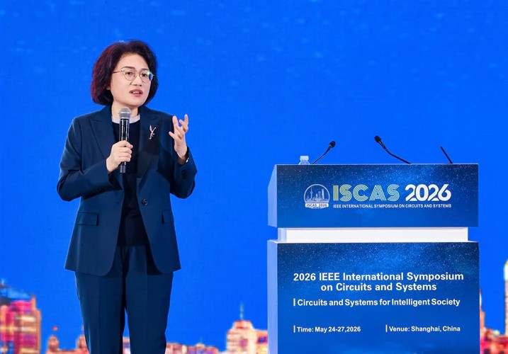
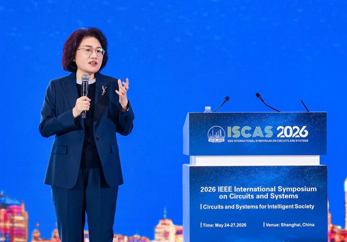
    Delivering a keynote address titled “New Semiconductor Path in Practice” at the 2026 IEEE International Symposium on Circuits and Systems (ISCAS), Huawei’s He Tingbo introduced the “Tau Scaling Law.” This new principle positions itself as a successor to traditional manufacturing paradigms, proposing a shift from physical geometric scaling—shrinking the physical size of transistors—to time scaling as the primary vehicle for driving next-generation electronic systems forward.

    For decades, the semiconductor industry has chased raw power by squeezing more transistors onto smaller silicon dies. However, as physics boundaries tighten and cost-per-transistor benefits erode, the industry has neared a critical bottleneck. Huawei’s Tau Scaling Law circumvents these physical limitations by focusing systematically on shortening the time constant $\tau$, compressing signal propagation delays to achieve massive efficiency gains rather than relying solely on traditional fabrication shrinks.

    To realize this leap in power, Huawei has established a multi-level co-optimization mechanism that spans the entire hardware stack, beginning at the foundational device layer. Here, engineers are optimizing the resistance and parasitic capacitance of transistors and interconnects to minimize delays at the underlying physical layer. At the circuit level, the framework introduces “LogicFolding” architecture, which shatters traditional physical layout boundaries to shorten critical-path wiring, slashing the resistive and capacitive loads that slow down signal propagation and boosting layout density.

    Moving higher up the stack, the chip-level design employs a full-stack coordinated strategy combining software, architecture, and silicon. This approach grants fine-grained, workload-driven control over instruction and data flows, which maximizes system-level parallelism and efficiency while cutting down end-to-end execution time. Finally, at the system level, Huawei is redefining interconnect protocols for massive computing systems with UnifiedBus, enabling unified memory addressing and native memory semantics for SuperPoDs to virtually eliminate communication latency.

    The technology is already moving rapidly from theoretical physics into commercial reality. Huawei revealed that it has spent the last six years designing and mass-producing 381 chips based on the Tau Scaling Law to seed various industry sectors. The upcoming Kirin smartphone chips, scheduled to debut in Fall 2026, will mark the first commercial deployment of the performance-boosting LogicFolding architecture. By 2031, Huawei projects that this temporal scaling methodology will allow its high-end chips to achieve an astronomical transistor density equivalent to a 14 A˚ (1.4 nm) process, securing a competitive, sustainable evolution path for high-performance AI and consumer computing.

    Recognizing the global scale of the silicon challenge, Huawei concluded the announcement with a call for international teamwork. He Tingbo emphasized that openness and collaboration remain key to driving ongoing progress, noting that no single company can independently find all the answers along the path of semiconductor evolution. With the launch of the Tau Scaling Law, Huawei aims to work closely with scientists, engineers, and industry partners around the world to drive the sustainable development of the broader electronics industry.

  • HUAWEI Introduces the Tau (τ) Scaling Law, Driving Advances in Transistor Density and System Performance

    HUAWEI Introduces the Tau (τ) Scaling Law, Driving Advances in Transistor Density and System Performance

    SHANGHAI, CHINA, MAY 26, 2026 – At the 2026 IEEE International Symposium on Circuits and Systems (ISCAS), He Tingbo of HUAWEI delivered a keynote speech titled “New Semiconductor Path in Practice”, unveiling the Tau (τ) Scaling Law as a new guiding framework for the future evolution of the semiconductor industry. The concept proposes a fundamental shift away from traditional geometric transistor scaling toward a time-based (τ) scaling principle, aimed at improving both semiconductor devices and electronic systems. Through this approach, technologies such as LogicFolding are introduced to reduce signal propagation delays and progressively increase transistor density, supporting continuous improvements in performance and efficiency.

    The proposal comes at a time when Moore’s Law, which has driven semiconductor progress for more than five decades, is facing increasing physical and economic limitations. As transistor scaling slows and cost efficiencies diminish, the industry is confronted with the need for a new sustainable path that can meet rapidly growing global computing demands. HUAWEI positions the τ Scaling Law as a response to these challenges, offering a new model for long-term technological advancement.

    Built on this principle, HUAWEI has developed core innovations such as LogicFolding and a multi-layer co-optimization strategy that spans devices, circuits, chips, and system architecture. At the device level, improvements focus on reducing resistance and parasitic capacitance to minimize time constants. At the circuit level, LogicFolding restructures traditional layouts to shorten critical paths and reduce signal load, improving both density and performance. At the chip level, integrated software, architecture, and silicon co-design enables more efficient workload handling and lower execution latency. At the system level, technologies such as UnifiedBus are used to reduce communication delays and enable more efficient memory and data management across computing systems.

    HUAWEI also highlighted real-world applications of the τ Scaling Law across smartphones and AI computing. According to He Tingbo, the company has already designed and mass-produced 381 chips using this framework over the past six years, supporting multiple industries and use cases. The upcoming Kirin chips, expected in Fall 2026, will be the first to adopt the LogicFolding architecture, promising significant performance gains. Looking further ahead, HUAWEI anticipates that its high-end chips by 2031 could achieve transistor densities comparable to 14 Å (1.4 nm) process levels through continued τ-based design evolution.

    In her keynote, He Tingbo also emphasized the importance of openness and collaboration in advancing semiconductor innovation. She noted that no single organization can solve all challenges in the industry alone, and called for deeper global cooperation among scientists, engineers, and industry partners. Through the τ Scaling Law, HUAWEI aims to contribute to a more sustainable and collaborative future for semiconductor and electronic system development.